
CoWoS, CoPoS, and CoWoP are so stupid that they can’t tell the difference. Who is the technology that the next generation should pay attention to?
As Moer's law gradually approaches the physical limit, the micro-condensation benefits of chip processing are limited, and the industry is seeking new breakthroughs, and Advanced Packaging has become one of the most popular technologies in recent years. As Taiwan's CoWoS production capacity gradually falls short of supply, new technologies such as CoPos and CoWoP have emerged in the world, but what is the difference between these two technologies and CoWoS? When will it start to be introduced? "New Science and Technology News" compiles relevant information and brings you to read it at once.
From the picture below, we can see that the stacking methods of CoWoS, CoPos, and CoWoP are actually somewhat different. For example, CoPoS mainly changes the intermediary layer to panel RDL; CoWop replaces the IC loader by developing PCB motherboards with higher technical content.
Next, we will introduce the main differences in these three technologies in detail, but before that, we must first understand the root of these extended technologies - TEU's advanced packaging CoWoS.
Taiwan Electric's advanced packaging technology CoWoS, which is further divided into CoWoS-S, CoWoS-R, and CoWoS-LCoWoS is 2.5D and 3D packaging technology of Telco, which can be divided into "CoW" and "WoS" to view.
CoW (Chip-on-Wafer) is a chip stack, and WoS (Wafer-on-Substrate) is a chip stack on the substrate. Therefore, CoWoS (Chip-on-Wafer-on-Substrate) means stacking the chips and then packaging them on the substrate. Finally, a 2.5D and 3D model is formed, which can reduce the space of the wafer and reduce power consumption and cost.
CoWoS is to first install the logical chip and HBM (high-frequency wide memory) on the silicon interposer, integrate the electronic signals of the left and right wafers through the tiny metal wires inside the interposer, and at the same time connect the lower substrate by silicon perforation (TSV), direct the signal downward, and finally connect the external circuit through metal balls (bumps).
Among them, CoWoS technology is divided into three technologies: CoWoS-R, CoWoS-L and CoWoS-S. Due to the different intermediary materials and costs, customers can choose which technology they want based on their own conditions.
The most expensive one is CoWoS-S, because the introductory layer uses "silicon" and is also a mainstream solution. For example, NVIDIA H100 and AMD MI300 both use CoWoS-S. However, due to the use of high-purity silicon and TSV processes, the processing difficulty is high, and the intermediary layer area is limited by the exposure machine, and the upper limit of the packaging size is about 2,500 square millimeters.
▲ CoWoS-S. (Source: TEK, the same below)
CoWoS-R uses the interconnect technology used in InFO, where the introductory layer connects to small wafers using RDL (re-text layer) to support elastic packaging design, suitable for cost-sensitive AI ASIC applications, network equipment or edge AI.
▲ CoWoS-R.
As for the cost of CoWoS-L is between CoWoS-S and CoWoS-R, the intermediary layer uses LSI (local Silicon Interconnect) and RDL, that is, local areas connect chips with silicon intermediary layer, and other areas use RDL or substrates to achieve dense chip connections and supports stacking applications up to 12 HBM memory, which can be said to combine CoWoS-S and CoWoS-R/InFO.
▲ CoWoS-L.
Hou Shangyong, the head of the Taiwan High-Efficiency Packaging Integration Office, mentioned in the Semicon Taiwan 2024 topic lecture that because the top die is very costly, CoWoS-L is the best solution that can meet all conditions better than CoWoS-R and CoWoS-S, so it will gradually move from CoWoS-S to CoWoS-L, and CoWoS-L is the blue-picture corner in the future.
Interestingly, some people believe that CoWoS-L means "Large", designed for ultra-large AI training platform and high-integration applications, extending the CoWoS-S architecture, but further breaks through the size limit of silicon intermediary layer and develops super-large area intermediary layer technology that can support more than 2,500 square millimeters.
▲ CoWoS technical route diagram. (Source: Compiled by new technology reports)
CoWoS "panelization"! Solve cost and large-size chip tumbling problemsAfter understanding the technical branches of CoWoS, let’s talk about CoPoS and CoWoP.
As AI chips become larger and more complex and their designs are becoming more complex, the traditional circular wafers are gradually limited in their area utilization and packaging efficiency, so they are beginning to "replace circles with squares", replacing the wafers with panels (Panels) and aligning the wafers on a rectangular substrate, and finally connecting them to the bottom layer of the loading board through the packaging process, so that multiple wafers can be packaged together, which is the so-called "CoPoS" (Chip-on-Panel-on-Substrate).
▲ CoPoS diagram. (Source: Yazhi Technology)
CoPoS is arranging chips on a square "panel RDL layer", replacing the original round silicon intermediary layer, strengthening the interconnection layout of different conductive layers and materials, and improving area utilization and production capacity. In addition, due to the introduction of new materials such as glass or blue stone, square sizes can be packaged with multiple wafers and integrate wafers of different sizes, and at the same time, it supports larger optical masks and solves the problem of larger wafers and becomes more obvious.
According to industry analysis, CoPoS is the "rectangular" deformation concept of CoWoS-L or CoWoS-R. It has changed the traditional 300 mm silicon circle to a square panel design, with dimensions of 310×310 mm, 515×510 mm or 750×620 mm, etc. Currently, the supply chain development directions are mainly based on the specifications of tyrene. However, the initial size selection of CoPoS is 310×310 mm.The industry has announced that Taiwan Electric plans to establish its first CoPoS experiment line in 2026, with the goal of realizing current production from the end of 2028 to 2029, and the first customer is NVIDIA. In addition, in the future, the direction of CoPoS packaging will mainly lock high-level applications such as AI, and will lock Broadcom, and CoWoS-L target services NVIDIA and AMD using CoWoS-R processes.
What is the difference between CoPoS and FOPLP (fan-out Panel Level Packaging)? The former is used for AI high-level chips and intermediary layer materials that are converted from silicon to glass, while the latter is used for mature processes of low-cost chips such as PMICs and RFICs. It does not require intermediary layers and is directly connected through RDL.
Cut off the packaging substrate and BGA, can CoWoP become the next main route of CoWoS?As for "CoWoP" (Chip-on-Wafer-on-Platform PCB), it is an advanced packaging route that has emerged this year.
The news comes from the Chinese media "Walker Street News", which is the content of NVIDIA's 12-year-old technical staff member Anand Mannargudi in the company's internal technology briefing. Currently released, NVIDIA will use two packaging technologies, including CoWoP and CoWoS, on the GR150 chips of the Rubin GPU series.
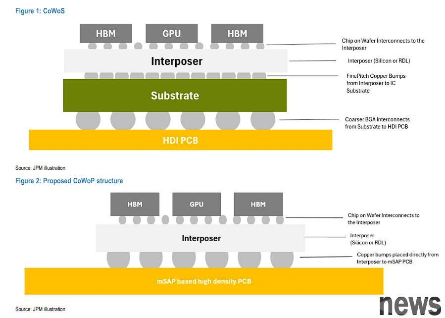
▲ CoWoP icon. (Source: Huaer Street Visit, JPM)
From the picture, we can see that CoWoS includes GPU and other logical ICs, HBMs, intermediary layers, and packaging substrates (Package Substrates), but in fact, the packaging substrate must be connected to the PCB motherboard (Platform PCB) through BGA (Ball Grid Array).
Because the CoWoS structure stacking is too high, it is stacking continuously like a building, but when the floor is higher, the longer the signal and power are transmitted from the bottom to the top floor, the higher the consumption and cost.
Therefore, CoWoP intends to remove some floors, that is, to directly cut off the expensive packaging substrate and BGA, and to develop a PCB motherboard with higher technical content, so that it can directly support high-precision signals and power supply cables, and then install the "chip and intermediary layer" combination directly on the PCB motherboard. In this way, the chip signal can go directly from the intermediary layer to the PCB motherboard, making the interconnection shorter, improving signal integrity, and better dissipation.
NVIDIA is currently testing CoWoP technology, and Taiwanese suppliers have also confirmed that the PCB motherboard that replaces ABF board has been officially sent to NVIDIA for testing.
▲ CoWoS, CoPoS, CoWoP technology progress. (Source: Compiled by new technology reports)
Wait, then what is WMCM technology?Although this time, it is mainly about CoWoS and its extended routes, there is also a "WMCM" (Wafer-Level Multi-Chip Module) this year, which is also worthy of attention, because Apple will launch the iPhone 18 in 2026, and its A20 processor will use this technology.
It is reported that WMCM is an upgraded version of TCM InFO-PoP, which is a packaging technology jointly developed by TCM and Apple and is a "Apple-specific" packaging technology.
InFO-PoP is to stack the memory directly above the mobile processor. When the memory capacity increases, heat dissipation becomes a problem. Therefore, WMCM is a way to replace traditional stacking with RDL by flatly encapsulating IC logical wafers and DRAM, replacing the intermediary layer with RDL.
▲ WMCM diagram. (Source: Investment in Ethan Youtube Screenshot)
Since WMCM integrates different components such as SoC and DRAM in the wafer round stage and then cuts into single wafers, there is no need to use an intermediary layer or substrate to connect the grains, which can improve heat dissipation and signal integrity.
▲ Comparison of InFO and WMCM technology. (Source: Technology News)
Extended reading: Taiwan Power CoWoS Production is in a hurry! The biggest winner of the military competition "Advanced Packaging Equipment Concept Stock" is a one-time view With the support of innovative differentiation technology, Shengmei semiconductor displays the complete product line energy of seven large panelsRecommend News
-
Rubin postponed to fight against MI450NVIDIA denies, AMD is still excited
-

Only cooperate but not invest? Japan Display How to reset the industry strategy?
-

Taiwan s per capita GDP this year is estimated to surpass Korea, and Korean medi
-
Delivery delays impact Q1 earnings report Supermarket plunged more than 9% after