
From heat to light! This new American invention "photon cooling" has greatly increased the computing efficiency of AI chips

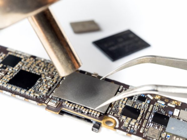
In today's high-performance chip designs, thermal management has become an increasingly severe challenge. Modern chips have billions of transistors inside them , but due to the existence of hot spots, these transistors cannot operate at the same time, causing up to 80% of the transistors to remain turned off. This phenomenon is called "dark silicon."
In order to solve this problem, Maxwell Labs, a new startup company in St. Paul, Minnesota, proposes a revolutionary technology: photonic cooling (photonic cooling). This technology can directly convert heat into light to achieve internal cooling of the wafer.
Maxwell Labs specializes in laser cooling technology. The company’s co-founder and chief growth officer Mike Karpe and CEO Jacob Balma play an important role in technology development. Traditional cooling methods, such as air and liquid cooling, rely mainly on moving heat away from the wafer surface, which faces bottlenecks at the high power density of future wafers. Maxwell Labs' photonic cooling technology places an ultra-pure gallium arsenide (GaAs) film cooling plate on top of the wafer, using lasers to precisely target hot spots for cooling. During this process, the laser irradiates the cooling plate, stimulating a phenomenon called anti-Stokes fluorescence, thereby achieving cooling.
The core of this technology lies in its ability to instantly detect hot spots on the chip and accurately point the laser at these hot spots, greatly improving cooling efficiency. Preliminary experiments show that the cooling capacity of this photonic cooling system is twice that of traditional air and liquid cooling systems, which will enable all functional units of the chip to operate simultaneously and solve the dark silicon problem.
In addition, photon cooling technology can also keep the operating temperature of the chip below 50°C, which will greatly increase the clock frequency of the chip and further promote the development of Moore's Law. Maxwell Labs’ research team is collaborating with institutions such as the University of New Mexico, Sandia National Laboratories, and the U.S. Army Research Laboratory to develop more efficient photon cooling materials, and plans to implement early applications in high-performance computing and artificial intelligence training clusters by 2027.
With the further development of photon cooling technology, future data centers will be able to significantly increase computing power and reduce energy consumption without increasing transistor density. This technology can not only change the design rules of chips, but may also become a key factor in promoting the advancement of computing technology.
You Can Cool Chips With Lasers?!?! A surprise contender for cooling computers: lasers Maxwell Labs, Sandia Collaborate to Test Laser-Based Cooling Tech Maxwell Labs Collaborates on Laser Cooling A surprise contender for cooling computers: lasers Maxwell Labs partners with Sandia National Labs for laser-based chip cooling Laser cooling breakthrough could make data centers much greener Laser-cooled GPUs get buy-in from the U.S. military — government beams cash to Maxwell Labs to cool AI processors Further reading: AI meets compound semiconductors, launching a materials revolution for high-performance computingRecommend News
-
Delivery delays impact Q1 earnings report Supermarket plunged more than 9% after
-
3Q25 NAND Flash contract price increased by 5% to 10%, weak demand for mobile ph
-

ASML will announce its Q3 financial report, and the market will focus on order m
-

Trump s course 100% Semiconductor tax responsibilities, legal persons are instru